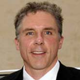
Harry Atwater
Founding Member, Kavil Nanoscience Institute
Thomas J. Watson Laboratory of Applied Physics
California Institute of Technology
MS 128-95
Pasadena, CA 91125
USA
Titles
- Howard Hughes Professor and Professor of Applied Physics and Materials Science, California Institute of Technology
- Founding Member, Kavil Nanoscience Institute
- Director, The Resnick Institute
Biography
Harry Atwater is currently Howard Hughes Professor and Professor of Applied Physics and Materials Science at the California Institute of Technology. His research interests center around two interwoven research themes: photovoltaics and solar energy; and plasmonics and optical metamaterials. Atwater and his group have been active in photovoltaics research for more than 20 years. Recently they have created new photovoltaic devices, including the silicon wire array solar cell, and layer-transferred fabrication approaches to III-V semiconductor III-V and multijunction cells, as well as making advances in plasmonic light absorber structures for III-V compound and silicon thin films. He is an early pioneer in surface plasmon photonics; he gave the name to the field of plasmonics in 2001. He has authored or co-authored over 200 publications, and his group’s developments in the solar and plasmonics field have been featured in Scientific American and in research papers in Science, Nature Materials, Nature Photonics and Advanced Materials.
He currently serves as as Director of the DOE Energy Frontier Research Center on Light-Matter Interactions in Solar Energy Conversion (http://lmi.caltech.edu) and was recently named Director of the Resnick Institute for Science, Energy and Sustainability, http://resnick.caltech.edu/, Caltech's largest endowed research program focused on energy. Atwater is founder and chief technical advisor for Alta Devices, a venture-backed company in Santa Clara, CA developing a transformational high efficiency/low cost photovoltaics technology, and Aonex Corporation, a compound semiconductor materials company. He has also served an editorial board member for Surface Review and Letters. Professor Atwater has consulted extensively for industry and government, and has actively served the materials community in various capacities, including Material Research Society Meeting Chair (1997), Materials Research Society President (2000), AVS Electronic Materials and Processing Division Chair (1999), and Board of Trustees of the Gordon Research Conferences. In 2008, he served as Chair for the Gordon Research Conference on Plasmonics.
Education
- PhD, Electrical Engineering, Massachusetts Institute of Technology, 1987
- SM, Electrical Engineering, Massachusetts Institute of Technology, 1983
- SB, Electrical Engineering, Massachusetts Institute of Technology, 1981
External Links
Journal Articles
2014
Deceglie, M. G., H. S. Emmer, Z. C. Holman, A. Descoeudres, S. de Wolf, C. Ballif and H. Atwater. 2014. Scanning laser-beam-induced current measurements of lateral transport near junction defects in silicon heterojunction solar cells. IEEE Journal of Photovoltaics 4(1):154-159. DOI: 10.1109/JPHOTOV.2013.2289353. (link )

